Základom skoro každého elektronického zariadenia je plošný spoj. Plošný spoj tvoria vodivé cesty medi priľnuté na nevodivom materiáli. Nespracovanému materiálu hovoríme cuprextit. Cesty sú vo finálnom stave poprepájané s elektronickými súčiastkami, ktoré vytvárajú rôzne elektronické obvody. 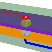 Na plošnom spoji môže byť jedna alebo viac vrstiev vodivých ciest. V miestach (v otvoroch), ktoré sú určené na prechod súčiastky z jednej strany na druhú, je celý prechod vodivý - tým sa zabezpečí prechod elektrického signálu z jednej strany plošného spoja na druhú (výnimkou sú SMD súčiastky, ktoré sa umiestňujú tak, že ich nohy ostávajú na tej istej strane, kde sú umiestnené – nie sú v otvoroch).
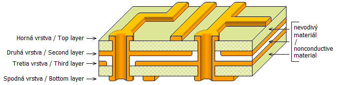
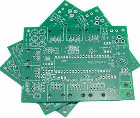 Jednoduché obvody majú vodivú vrstvu len na jednej strane (na jednej sú vodivé cesty a na druhej súčiastky), zložitejšie na oboch stranách, či vo viacerých vrstvách nad sebou oddelených nevodivou vrstvou. V miestach, kde je potrebný prepoj medzi vrstvami sa vytvorí prechodový otvor, ktorý je vodivý. V našej modernej dobe sa všetko miniaturizuje a preto sa vývojári snažia implementovať veľké množstvo elektroniky na malý kus výrobku (tu musia byť dvoj a viacvrstvové dosky plošných spojov). Na to, aby plošný spoj bol plošným spojom, sa musí vyvinúť a následne vyrobiť. Je viacero technologických postupov, ktoré sa využívajú na takúto výrobu. Skrátene to môžeme zhrnúť napríklad takto:
- Návrh schémy elektronického obvodu
- Návrh plošného spoja a tvorba šablón ako podklad do výroby
- Výroba, ktorá môže mať mnoho fáz a rôzne technologické postupy - napr.:
- nanášanie odolnej vrstvy voči leptaniu žieravinou z predlohy šablóny
- samotné leptanie v žieravine (alebo vývojke – pri inom technologickom postupe)
- rôzne čistiace procesy, vŕtanie, gravírovanie
- pocínovanie, nanesenie rôznych ochranných a označovacích vrstiev
- elektronická a optická kontrola
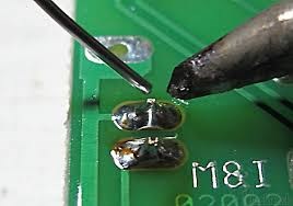
- Osadenie elektronických súčiastok automatickým robotom, alebo ručne (pri špeciálnych súčiastkach)
- Kontrola a test celého osadeného obvodu na danej doske
Pochopiteľne je možné si dosku plošného spoja vyrobiť aj v domácich podmienkach. Technologických postupov je mnoho. Tu je jeden príklad (link).
Na Slovensku máme v súčasnosti veľmi kvalitné výrobne takýchto dosiek, ktoré podliehajú a plnia požadované normy (napr.: RoHS – bezolovnatý produkt). Niektoré ponúkajú celý proces od vývoja a návrhu po samotné osadenie a test finálnej dosky vrátane súčiastok. Na nasledujúcej stránke sú videá s názornou výrobou plošných spojov : (link).
Niečo o týchto doskách máme aj na Wikipedii: SK alebo EN.
The basis of almost every electronic device is a printed circuit board. PCB form a conductive path of copper adhering to the non-conducting material. Unprocessed material we talking cuprextite. Roads are in the final state intertwined with electronic components that produce various electronic circuits.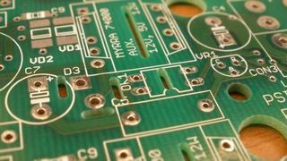 On the printed circuit board may be one or more layers of conductive paths. In places (in the holes), which are designed to switch parts from one side to the other, is the entire conductive passage - by facilitating the transition of an electrical signal from one side of the printed circuit board to the other (except for SMD components, which are placed so that their legs remain on the same side, where they are located - not in the holes).
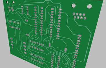 Simple circuits have a conductive layer on only one side (the one on the conductive path and the other components), more difficult circuits on both sides, and in several layers one above the other separated by non-conductive layer. In the places where is the jumper between the layers needed, will creates a through hole which is conductive. In our modern times, is everything miniaturizes and therefore developers trying to implement a large number of electronics on a small piece of the product (there must be two-and multilayer printed circuit boards). In the order, for the printed circuit board to be printed circuit board, has to be applied and subsequently produced. There are several techniques, which are used for such manufacture. At a glance it can be summarized like this:
- The electronic circuit design of the scheme
- PCB design and creation of templates as a base to manufacture
- Production, which can have many stages and various processes like.:
- the application of layer resistant to caustic etching of a master template
- the actual etching in alkali (or developer - for a technological process)
- the various cleaning processes, drilling, engraving
- the tinning, applying various protective layers and marking
- the electronic and optical inspection
- Replacing electronic components by automatic robot or manually ( for special components)
- Inspection and test the entire circuit by fitting the board
Obviously it is possible to make the circuit board at home. There are many Technological techniques.
 There are very good producers of such boards, in Slovakia. These complies with the required standards (eg RoHS - unleaded product). Some of the producers offer the entire process from development and design to the actual casting and final test boards including parts. On the next page are videos with illustrative PCB: (link).
There is something about the boards also on Wikipedia: SK or EN.
No a teraz ku keške ! Na zadaných (úvodných) súradniciach kešku nehľadajte !!!
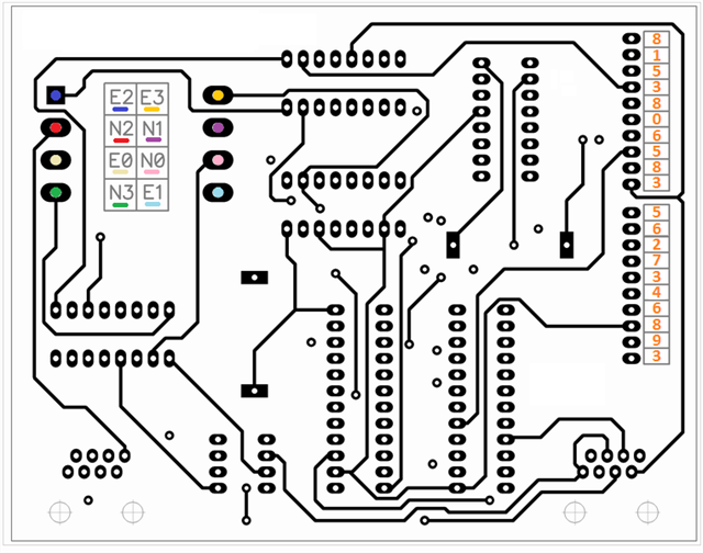
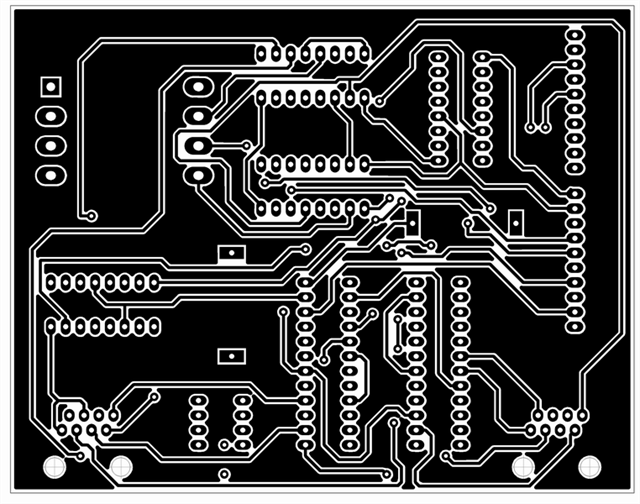
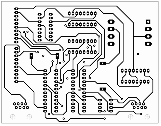
Na nasledujúcich obrázkoch máme vymyslenú takúto dosku plošného spoja (nejedná sa o žiadny produkčný návrh). Prevedením sa jedná o trojvrstvovú. Finál je na súradniciach:
N48° 1(N0).(N1)(N2)(N3), E017° 0(E0).(E1)(E2)(E3).
Príjemnú zábavu.
And now to the cache! Don’t look for the cache on the assigned (initial) coordinates!!!
The following figures is imagined such a circuit board (this is not production design). Converting is a three-layers. Finale is at coordinates N48° 1(N0).(N1)(N2)(N3), E017 0(E0).(E1)(E2)(E3).
Have a fun.
 GeoChecker ---->
  <---- GeoChecker